With each GF11x GPU effectively being a half-step above its GF10x predecessor, NVIDIA’s replacement strategy has been to split a 400 series card’s original market between two GF11x GPUs. For the GTX 460, on the low-end this was partially split off into the GTX 550 Ti, which came fairly close to the GTX 460 768MB’s performance. The GTX 460 1GB has remained in place however, and today NVIDIA is finally starting to change that with the GeForce GTX 560. Based upon the same GF114 GPU as the GTX 560 Ti, the GTX 560 will be the GTX 460 1GB’s eventual high-end successor and NVIDIA’s new $200 card.
| GTX 570 | GTX 560 Ti | GTX 560 | GTX 460 1GB | |
| Stream Processors | 480 | 384 | 336 | 336 |
| Texture Address / Filtering | 60/60 | 64/64 | 56/56 | 56/56 |
| ROPs | 40 | 32 | 32 | 32 |
| Core Clock | 732MHz | 822MHz | >=810MHz | 675MHz |
| Shader Clock | 1464MHz | 1644MHz | >=1620MHz | 1350MHz |
| Memory Clock | 950MHz (3800MHz data rate) GDDR5 | 1002Mhz (4008MHz data rate) GDDR5 | >=1001Mhz (4004MHz data rate) GDDR5 | 900Mhz (3.6GHz data rate) GDDR5 |
| Memory Bus Width | 320-bit | 256-bit | 256-bit | 256-bit |
| Frame Buffer | 1.25GB | 1GB | 1GB | 1GB |
| FP64 | 1/8 FP32 | 1/12 FP32 | 1/12 FP32 | 1/12 FP32 |
| Transistor Count | 3B | 1.95B | 1.95B | 1.95B |
| Manufacturing Process | TSMC 40nm | TSMC 40nm | TSMC 40nm | TSMC 40nm |
| Price Point | $329 | ~$239 | ~$199 | ~$160 |
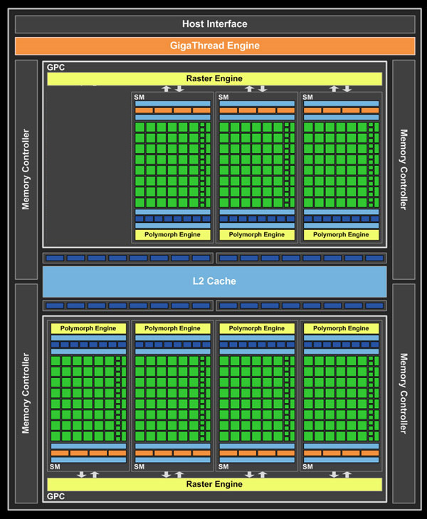
The GTX 560 is basically a higher clocked version of the GTX 460 1GB. The GTX 460 used a cut-down configuration of the GF104, and GTX 560 will be doing the same with GF114. As a result both cards have the same 336 SPs, 7 SMs, 32 ROPs, 512KB of L2 cache, and 1GB of GDDR5 on a 256-bit memory bus. In terms of performance the deciding factor between the two will be the clockspeed, and in terms of power consumption the main factors will be a combination of clockspeed, voltage, and GF114’s transistor leakage improvements over GF104. All told, NVIDIA’s base configuration for a GTX 560 puts the card at 810MHz for the core clock and 4004MHz (data rate) for the memory clock, which compared to the reference GTX 460 1GB is 135MHz (20%) faster for the core clock and 404MHz (11%) faster for the memory clock. NVIDIA puts the TDP at 150W, which is 10W under the GTX 460 1GB.
Read More - http://www.anandtech.com/show/4344/nvidias-geforce-gtx-560-top-to-bottom-overclock
No comments:
Post a Comment